Log in using the credentials which you just set earlier while signing up.
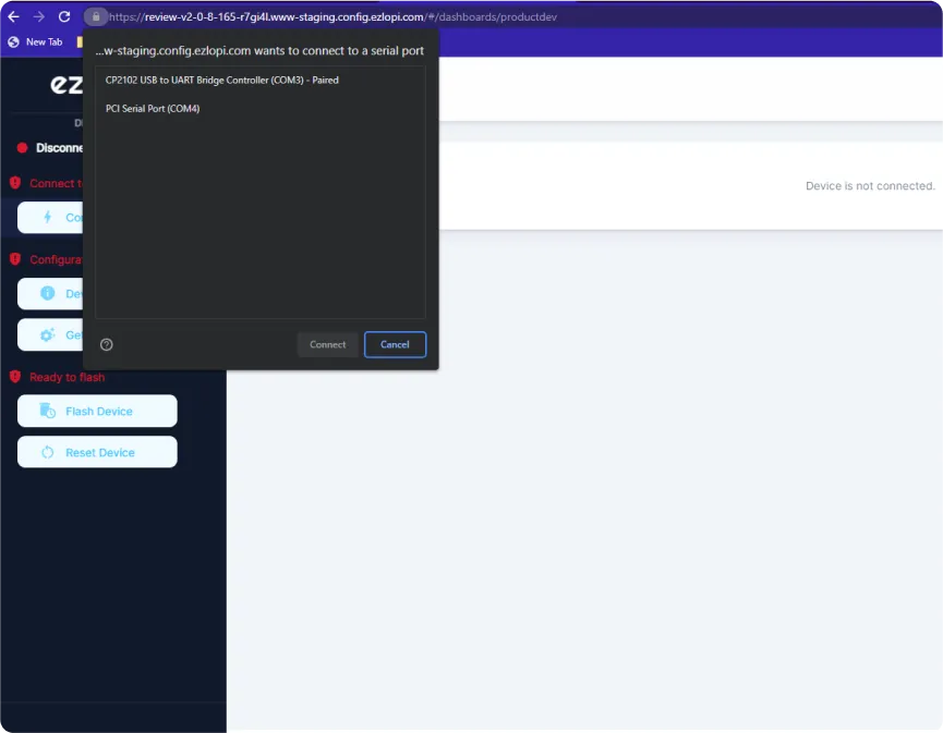
Now click on Connect Device and a pop-up window will appear
Now, select COM Port to which your ESP32 device is connected. In our case, the COM3 port is used.
Click Connect
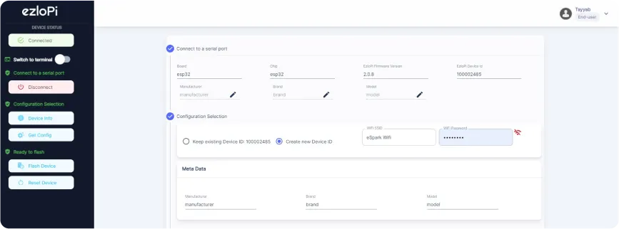
If you are new to this and it’s your first time configuring, select Create new Device ID. Enter Wifi SSID and Wifi Password.
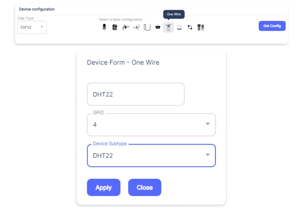
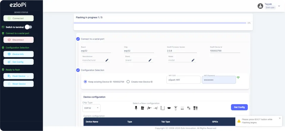
In the Device Configuration, tab click on One Wire.
A pop up window will open for inputting the following parameters.
Set a device name of your choosing. In our case we set it to DHT22
Set Out GPIO to 4.
Select The Device Subtype as the sensor you are choosing. In our case, we set it to DHT22.
Now Click the Apply button.
After clicking the apply button you can see a table of your setting in the device configuration tab. Press the Flash Device button.
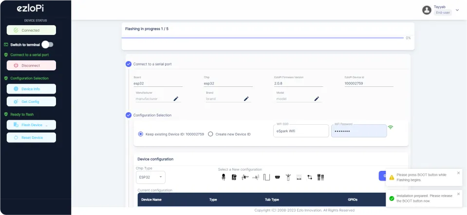
A window will appear on the bottom left side of the screen displaying “Please press BOOT button while flashing begins.”
Hold the BOOT button down until the next window appears on the bottom left side of the screen which says “Installation prepared. Please release the boot button now.”
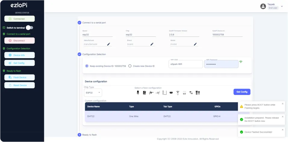
Release the BOOT button from your ESP32 when this pop-up on the bottom right window appears.
After some time this popup will appear saying Device Flashed Successfully! This means that your device has been set up successfully.
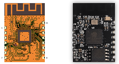
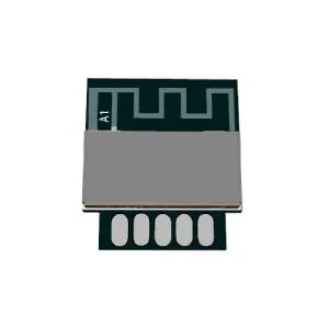
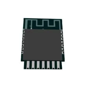
Ezlo_EP01
Ezlo_EP01 is a low-power embedded Wi-Fi and Bluetooth module that Ezlo has developed. It consists of
a highly integrated chip (ESP32-D0WDQ6), a few peripherals, an embedded Wi-Fi network protocol stack,
the Bluetooth LE network protocol, and varied library functions
1.Overview
The Ezlo_EP01 is a versatile Wi-Fi+Bluetooth®+Bluetooth LE MCU designed for a wide range of
applications, from low-power networked sensors to the most challenging tasks such as voice encoding,
music streaming and MP3 decoding. This module is based on the ESP32-D0WDQ6* chip. The embedded
chip is designed to scale and adapt.
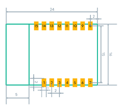
Ezlo_EP01 has two rows of pins with a 2 ±0.1 mm pin spacing. The Ezlo_EP01 dimensions are 16 mm (W)×24
mm (L) ×1.2 mm (H). The diagram of dimensions
2.2 Pin definition
1 – Gpio21
(ADC AI)
2 – En
(I – Enabling pin, which needs to be connected to the voltage of 3.3V in normal cases and corresponds to CHIP_EN)
3 – Gpio25
(I/O – Common IO pin)
4 – Gpio26
(P – Support hardware PWM)
5 – Gpio27
(I/O – Support hardware PWM and Common IO pin)
6 – Gpio16
(I/O – Support hardware PWM and Common IO pin)
7 – Power+3,3V
(P – Power supply source (3.3V))
8 – Gnd
(P – Power supply reference ground)
9 – Gpio19
(O – Common IO pin)
10 – Gpio22
(O – Common IO pin)
11 – Gpio4
(I/O – Common IO pin)
12 – Gpio17
( I/O – Support hardware PWM and Common IO pin)
13 – Gpio23
( I/O – Support hardware PWM and Common IO pin)
14 – Rx1
(I/O – UART0_RXD)
15 – Tx1
(I/O – UART0_TXD)
3. Electrical parameters
3.1 Absolute Maximum Ratings
Parameter
Description
Min
Max
Unit
VDDA, VDD3P3, VDD3P3_RTC,
VDD3P3_CPU, VDD_SDIO
Allowed input voltage
–0.3
3.6
V
Ioutput
Cumulative IO output current(1)
—
1200
mA
TSTORE
Storage temperature
–40
150
°C
*The product proved to be fully functional after all its IO pins were pulled high while being connected to
ground for 24 consecutive hours at ambient temperature of 25 °C.
Recommended Power Supply Characteristics
Parameter
Description
Min
Typ
Max
Unit
VDDA, VDD3P3_RTC ,
VDD3P3, VDD_SDIO (3.3 V mode)
Voltage applied to power supply pins per power domain
2.3/3.0
3.3
3.6
V
VDD3P3_CPU
Voltage applied to power supply pin
1.8
.3.3
3.6
V
IVDD
Current delivered by external power supply
0.5
–
–
A
T
Operating temperature
–40
—
125
°C
3.2 DC Characteristics (3.3 V, 25 °C)
Parameter
Description
Min
Typ
Max
Unit
CIN
Pin capacitance
—
2
—
pF
VIH
High-level input voltage
0.75×VDD
—
VDD+0.3
V
VIL
Low-level input voltage
–0.3
—
0.25×VDD
V
IIH
High-level input current
—
—
50
nA
IIL
Low-level input current
—
—
50
nA
VOH
High-level output voltage
—
—
—
V
VOL
Low-level output voltage
—
—
0.1×VDD
V
IOH
High-level source current
VDD3P3_CPU power domain
(VDD1 = 3.3 V, VOH >= 2.64 V
VDD3P3_RTC power domain
output drive strength set to the maximum)
VDD_SDIO power omain
—
—
—
40
40
20
—
—
—
mA
mA
mA
IOL
Low-level sink current (VDD1= 3.3 V, VOL = 0.495 V, output drive strength set to the maximum
—
28
—
mA
RPU
Resistance of internal pull-up resistor
—
45
—
VkΩ
RPD
Resistance of internal pull-down resistor
—
45
—
VkΩ
VIL_nRS
Low-level input voltage of CHIP_ PU to shut down the chip
—
—
0.6
V
3.3 RF Current Consumption in Active Mode Current Consumption Depending on RF Modes
Work Mode
Min
Typ
Max
Unit
Transmit 802.11b, DSSS 1 Mbps, POUT = +19.5 dBm
—
240
—
mA
Transmit 802.11g, OFDM 54 Mbps, POUT = +16 dBm
—
190
—
mA
Transmit 802.11n, OFDM MCS7, POUT = +14 dBm
—
180
—
mA
Receive 802.11b/g/n
—
95 ~ 100
—
mA
Transmit BT/BLE, POUT = 0 dBm
—
130
—
mA
Receive BT/BLE
—
95 ~ 100
—
mA
3.4 Wi-Fi Radio Characteristics
Parameter
Description
Min
Typ
Max
Unit
Operating frequency range
—
2412
—
2484
MHz
Output impedance
—
—
30+j10
—
Ω
TX power
11n, MCS7
11b mode
12
18.5
13
19.5
14
20.5
dBm
dBm
Sensitivity
11b, 1 Mbps
11b, 11 Mbps
11g, 6 Mbps
11g, 54 Mbps
11n, HT20, MCS0
11n, HT20, MCS7
11n, HT40, MCS0
11n, HT40, MCS7
—
—
—
—
—
—
—
—
–98
–88
–93
–75
–93
–73
–90
–70
—
—
—
—
—
—
—
—
dBm
dBm
dBm
dBm
dBm
dBm
dBm
dBm
Adjacent channel rejection
11g, 6 Mbps
11g, 54 Mbps
11n, HT20, MCS0
11n, HT20, MCS7
—
—
—
—
27
13
27
12
—
—
—
—
dBm
dBm
dBm
dBm
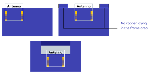
4. Antenna
4.1 Antenna type
Ezlo_EP01 uses only an onboard PCB antenna.
4.2 Antenna interference reduction
To ensure optimal Wi-Fi performance when the Wi-Fi module uses an onboard PCB antenna, it is recommended that the antenna be at least 15 mm away from other metal parts. To ensure antenna performance, the PCB should not be routed or clad with copper in the antenna area.
The main points of the layout: Make sure that there is no substrate medium directly below or above the
printed antenna. Make sure that the area around the printed antenna is far away from the metal copper skin,
so as to ensure the radiation effect of the antenna to the greatest extent
5 Recommended PCB layout
6 Power-on sequence and resetting
6.1 Treatment of GPIO pins
A few pins of the module will have instantaneous high-level pulses before the chip fully works, and
everything will be normal after the chip works. For these pins, if they are directly used as driving light
sources or relays, in order to avoid the effect of burrs at the moment of power-on, refer to the following
processing methods: Pull down a 1-KΩ resistor at an output port of a pin, and then connect a diode in
series. At this time, the voltage of a GPIO will drop to about 2.7V after passing through the diode. The red box
represents the original drive tube on the customer’s baseboard. A diode D1 and pull-down 1-KΩ resistor
need to be added. If a lamp is directly driven, pull down a 10-KΩ resistor on the grid of the positive Mos.
If a lamp is not directly driven and a PWM signal will not be sent until the module is officially launched,
there is no need to add a pull-down resistor and diode. If a relay is driven, you can change the diode to
a resistor of 0 Ω according to the actual situation.
6.2 Storage Conditions
The products sealed in moisture barrier bags (MBB) should be stored in a non-condensing atmospheric
environment of ∠ 40 °C and 90%RH. The module is rated at the moisture sensitivity level (MSL) of 3.
After unpacking, the module must be soldered within 168 hours with the factory conditions 25 ± 5 °C and
60 %RH. If the above conditions are not met, the module needs to be baked.
6.3 Electrostatic Discharge (ESD)
Human body model (HBM): ±2000 V
Charged-device model (CDM): ±500 V
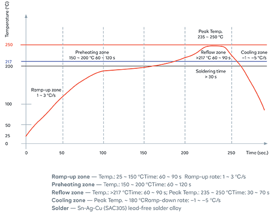
6.4 Reflow Profile
Solder the module in a single reflow
6.5 Ultrasonic Vibration
Avoid exposing Ezlo_EP01 modules to vibration from ultrasonic equipment, such as ultrasonic welders or
ultrasonic cleaners. This vibration may induce resonance in the in-module crystal and lead to its
malfunction or even failure. As a consequence, the module may stop working or its performance may
deteriorate